Available equipment includes:
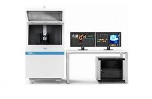
Park NX20 AFM
The NX20 is one of the most accurate large-sample AFMs available. It provides high precision and resolution and includes a true non-contact mode. It has a number of unique features and a user-friendly design that makes it ideal for less experienced AFM users. The unit in the lab is fitted with all the optional components to allow a wide range of measurement types.
- Sidewall measurements for 3D structure study
- Surface roughness measurements
- High resolution electrical scan mode
- Kelvin probe force microscopy
- All optional scan modes installed
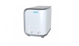
JEOL JCM-6000 SEM
This benchtop SEM is a multi-functional tool that offers quick turnaround images. The magnification far exceeds the capabilities of optical microscopes. It is easy to use, with many operations handled automatically. This unit is fitted with the elemental analysis device.
- Benchtop scanning electron microscope
- High and low vacuum modes
- Length measurement functions
- Elemental analysis (EDS) installed
- Images within 3 minutes of power on


